
Tags and keywords
All pins on the 2nd header of the Mega2560 only involve the ATmega2560 mcu chip or the GND and +5V nets:
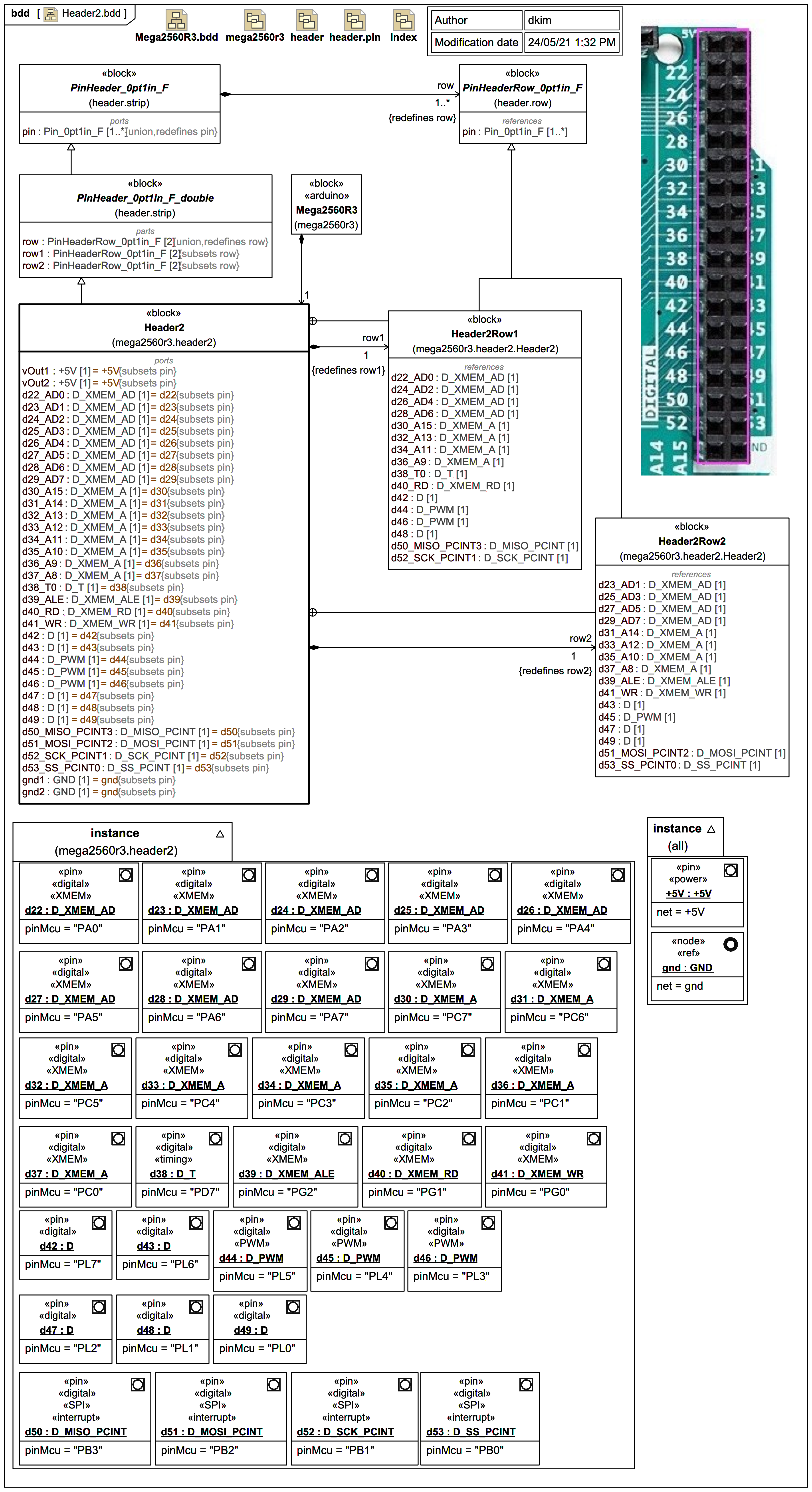
Apart from most pins acting as digital I/O pins, the 2nd header also offers access to:
- 16 pins for the XMEM expansion points to additional external SRAM, split into 8 pins for multiplexed data and low order address, and 8 high order address pins.
- A T0 timer pin.
- An XMEM Address Latch Enable (ALE) pin
- An XMEM inverted read strobe RD pin
- An XMEM inverted write strobe WD pin
- 3 additional Pulse Width Modulation (PWM) pins
- Serial Peripheral Interface (SPI) Pins (MISO, MOSI, SCK, SS)
The pin ports in the header block have corresponding pin shared reference properties split across the 2 row blocks, but we won't be using the row blocks further in this trail.
Separate system-wide instances of type GND and +5V with net values (rather than a mapping to a specific pin), have been assigned as Context-Specific Values for pins of corresponding types.